Great to hear that!!
I use Highcharts for the graphs, it’s awesome and free for private use. You can do almost everything with, the limit is imagination.
I played around and added night/day shadow, min/max , etc…
You’re certainly right, the HX712 doesn’t bring anything if the 256gain factor can’t be used. It has some advantage though, but knowing what i know now, i would probably not use it again.
Anyway, it works now and the datas coming out are stable.
I did put 4 converters, so anyone can use it how he wants. 1 cell/hive or any other combination.
Hm… REFP is at least not allowed to be higher than AVDD, lower and equal is valid. If you would feed your gauges via the internal high-side FET switch, the voltage drop is RDSon * Igaugedrain , e.g. the FET in the HX712 has nom. RDSon=3 Ohm, your gauge wants 20mA, then @AVDD=5V REFP will be 60mV lower (if you short R3, R4 in typ. schema in datasheet page 1) - so REFP in most usages will be lower than AVDD, but is allowed to be equal to AVDD, if we belive in the data sheet on this…
They claim:
When internal MOS power switch is used for the external load-cell, both HX712 and the load-cell will be powered down.
I suppose that the digital part of the HX712 then still is powered, othwerwise normal function could not be reestablished by PD_SCK - the data sheet here is as inaccurate as most Chinese IC documentation.
This is most likely the result of back-feeding - the sink BAT (the second, single-ended ADC input) became a source via the internal protection diodes because of your void case REFP > AVDD.
1 Like
Hi Weef,
Thanks for the comments…
I learned it the hard way ! I started using the chinese datasheet as Aviac didn’t give an english version on their site, only a short presentation. I requested it, but never got an answer. I also told them that the HX711 datasheet had an error…
I found the HX712 english version of the datasheet later on, but it still is not on their Web page !
I used Google translate and the chinese version does not say the same about the BAT input. It claims that it has to be connected to DVDD if not used, what i did.
And yes, DVDD is always supplied.
This is most likely the result of back-feeding - the sink BAT (the second, single-ended ADC input) became a source via the internal protection diodes because of your void case REFP > AVDD.
That makes sense… But as already mentionend, the chinese datasheet is telling the contrary… As i do switch the external AVDD source (to save the power regulator quiescent current) and firstly connected BAT to AVDD, it was causing problems… For now, i left it unconnected and it does not harm
Now, i’m facing another problem i discovered yesterday evening.
I wired 2 HX712 on my board, and my software is measuring one cell after the other. When i measure the first time, it is OK. The second time, the datas are completely weird. I tracked it and found out that it happens only when i measure the second HX712 …
It is like if when the power on AVDD disappears, it create problems when repowered ON and no measure is done…
I have to confirm this.
Adding the fact that i can’t use the 256 gain, it was probably not a good idea to use these chips !
The safest way to use these chips is to use the internal switch, leave the AVDD stable and the BAT on this pin. Everything i wanted to avoid, for power saving and noise reinjection on the AVDD line !
I will drop a mail to Aviac and ask for some details and if the batch of ICs i have have problems or not…
Not sure if they will answer.
Thanks for the help.
I finaly found out that if the AVDD doesn’t appear long enough before the chip is waked up, it produces garbage.
So, i modified my board with some track cuts and wires. I now have the 5V low noise regulator working permanently and this 5V is applied to the AVDD pins of all HX712. The OUT pin is now connected the REFP and the cell.
The BAT input is left unconnected as there is no interest for me, being powered on a 12V battery.
Evrything works fine now and as expected, except the 256 gain setting that does not work.
They twice in the manual want us it to
(connect to higher of AVDD or DVDD when not used)
But, anyway,
When detecting battery input, AVDD is used as the ADC’s data conversion reference voltage.
…and not REFP; their internal switched voltage divider on BAT ‘sees’ AVDD as ref. That’s also why they could allow BAT being connected to the "Regulator"s input and having AVDD and DVDD behind (in their reference PCB design)… funny data sheet.
As BAT does not refer to REFP but AVDD, it makes is useless for precise measurement of the weight scale element voltage source (if (BAT conn’d w/ REFP) AND (REFP different to AVDD)). So, then … connect it “to higher of AVDD or DVDD when not used” ;)
That is good to hear!
let’s see what this finally will be…
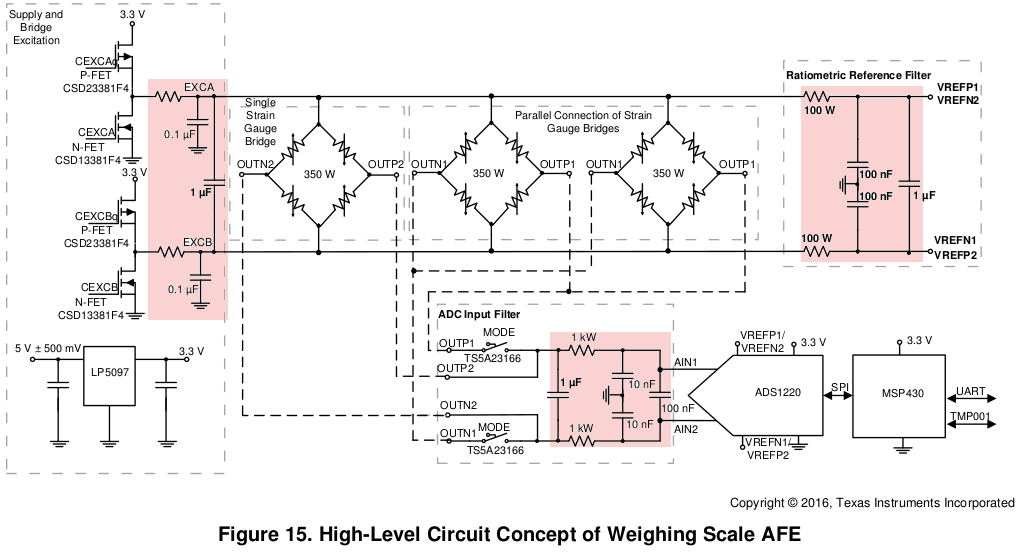
You seem to really need this high PGA gain @24bit - then consider implementing these simple RC networks (or ferrites instead R w/ adequate DC res, if your GSM modem+antenna are close) as shown in this app note from TI (coloring by me, local pdf linked here) - it helps signal, reference and sensor supply conditioning even at lower gains! ;)
(my pdf renderer obviously shows “Ohm” as “W”)
1 Like
Hi Weef,
Thanks for all these technical infromations.
Yes, the datasheet is really unclear concerning this BAT input. I find it useless, with a gain factor 1 and such an input voltage divider, it only can be used to detect the presence of a voltage.
Just for fun, i will try to connect it to the 5V line and see if there is a difference.
I personally don’t need a gain of 256, having standard 2mV/V cells. But i thought i could use these chips and someone can connect lower ouput voltage cells. But it seems that, at least the batch i have, they can’t be switched to 256 !
My board has the filtering on inputs and supply you suggest. I have the resistors and caps at AN1 and AN2 and implemented the 100 Ohms on the REFP and EFN lines. I don’t have 1uF caps though… only 0.1uF
I had to remove the 100 Ohms, due to the hacks i had to make on my pcb… I didn’t try to see if the voltage drop through these 100 Ohm would affect the measures. Any idea ?
For the moment tracking my other problems, i shorted the 1kOhms in the input. I will remove the shorts and try with the 1kOhms.
I wanted to have as much voltage i could on the cells, and that’s why i added the 5V regulator. It makes some difference over a HX711 with internal regulator and their 2,45V output…
BTW, the LT1761 i use has quite low quiescent current, so leaving it working all time to avoid timing problems doesn’t make a big difference. Actually with the Pro mini, the DS3231, the DS18B20 sensors and the BME280, i have about 320uA when in sleep.
I suppose that i could reduce it in changing the RTC DS3231 for another one, as the datasheet says it has 110 uA standby current. But that’s another story…
The GSM itself consumes a lot more during the short period it transmits.
Thanks for you help,
Patrick.
In contrary to what i thought, i got an answer from Avia to my questions about the HX712.
But this answer is quite disappointing !
The HX712 DOES NOT have a gain of 256 possibility !! So, there is no reason to use it over the HX711.
Sorry to hear that…
Here the answer from Avia :
…
Hi,
This batch is coming from our factory. HX712 can’ t be used at a gain of 256.
Thank you.
Best regards,
Mandy
海芯科技(厦门)有限公司
AVIA SEMICONDUCTOR (XIAMEN) CO. , LTD.
ADD: 301E NO. 34 Guanri RD, Xiamen Software Park Ⅱ, Xiamen, China
Tel: 0592-2529530
Fax: 0592-5996329
Thanks, Patrick, for this information! May you ask Avia about an official datasheet.
We found a datasheet, I don’t know the source, see:
https://community.hiveeyes.org/uploads/default/original/1X/35591ec403137b7dc1c70d451b339942f0def3fd.pdf that claims as feature:
On-chip low noise PGA with selectable gain of 128 and 256
Is this an error in the documentation or not implemented in the current batch only and will be available in the future for the HX712?
Hi Clemens,
Here is what they answered when i told them that they should modifiy their datasheet :
Hi Patrick,
We are sorry that we don’ t modify the datasheet in time. We will revise it.
Sorry again.
Best regards,
Mandy
海芯科技(厦门)有限公司
Well, this datasheet can be found since many years… I don’t know what they’re playing. In any case, that’s not serious !
It started to be a good product, but now it looks more like a reworked HX711… It’s still a nice chip to use, but not as expected.
Hey there,
for the sake of completeness, let me reference the conversations with Bogdan, the author of the HX711 library started by Patrick (@TK5EP, @GitHub) the other day on GitHub:
https://github.com/bogde/HX711/issues/39
https://github.com/bogde/HX711/issues/91
Cheers,
Andreas.
Understood.
this I don’t get: HX711’s band gap VBG is 1,25V, VSUP starts @2,7V… but: Where does this 2,45V come from? Don’t you use an external PNP and incorporate the ‘LM317-style’ LDO in the HX711 for sourcing the cell (and AVCC)?
How dare you! ;) You do want to drop an RTC/TCXO which gives you 2ppm worst case over full industrial temp spec, resulting in less than 2 minutes off per year, don’t you?! Any chinese counterfait or ‘ghost-shift’ DS3231 is way better than a DS13x7 or the like. Your design already incorporates this IC part, and it is perfect for a node having a WWAN link itself and no local gateway providing the link as well as accurate system time stamps).
110uA is only true when
- VCC is used as the primary source and
- the DS3231 does not run from VBAT.
If VCC= 0V and VBAT >= 2,3V, the the 3231 lives on a timekeeping ‘battery’ current IBATT as low as typ 1uA, max 3,5uA!
In the data sheet, note 5 on this says:
Current is the averaged input current, which includes the temperature conversion current.
This is the current requirement when running only on VBAT:
(from here; this ‘app note’ is mostly advertisement for DS3232/3234)
So, by sourcing the DS3231 via a GPIO pin (and RV + decoup caps to make this ‘switch’ low-impedance) and using VBAT most of the time (similar to that), you can achieve an averaged one-digit uA drain for the DS3231. You still can wake up the processor via INT by RTC alarms (see INTCN, A1IE (A2IE) and BBSQW bits).
I’m not familiar with the DS3231M (nor DS3232(M), DS3234) which has different entrails (they don’t mention a TCXO anymore but a TC MEMS resonator…that’s why the SO8 packages was feasible).
Before going deeper into DS3231-related things (which would need me to open a new thread ;) ), I’d point to a very comprehensive entry on this, esp. the update on 2014-10-28 - it also discusses the cheap chinese ‘versions’ of the DS3231 in terms of origin and accuracy, and this guy runs great long-term series:
1 Like
Hi !
A happy new year to all on this forum ! A prosperfull beekeeping and building.
@weef
The 2.45V is what i had in memory when i tested these chinese HX711 boards. I have to check on one to confirm if this was the voltage i found on the cell…
Yes, as far as i remember, my prototype is using the on board PNP to switch a 5V supply. I can’t remember if i used this PNP to switch the output voltage or the ENABLE pin of a regulator. I think it’s this later solution.
My fault… i didn’t redraw the schematic after all my tests. I trusted my memory which i shouldn’t do anymore ! :-(
Thanks for the link to the datalogger. I already came across.
I modified my sketch and desactivated the A/D converter and brown-out, and my current dropped to 150uA.
I don’t have a spare digital pin to try to supply the DS3231. I will try to find a solution. But 'im not sure if it’s really worth it. The GSM is consuming a lot more each hour !
BTW, i was talking of a replacement for the DS3231 like the PCF2127 not a DS1307.
I’m actualy using 2 pins for each HX712. To free some pins, it might be possible to use one common pin for all four DOUT signals and one pin for each of the PD_SCK lines.
But i’m not sure it’s a good solution… It would wake up all 4 chips at the same time and supply all cells, consuming much more…
Have you made some tests with the DC filters you suggested ? What about the voltage drop across the resistors ?
Thanks a lot,
@TK5EP:
Hi Patrick,
I see you are using the HX712 chip. I also ordered a couple of bare chips and dug into the data sheet. As already mentioned there seem to be a couple of unclear sections (one might deduct that the chip is not able to be set to a gain of 256 since it never appears in the electrical characteristics :( - although it is stated in the reading protocol. But before jumping into the details:
Does the HX712 give you any (real?) advantages over the HX711 (temp stability, etc?).
Now a couple of detailed questions:
-
I am struggling to set the correct AVDD and DVDD voltage (3.3V)? AV shall be <= DV … well Do you use an external voltage divider (as with the HX711 or not). In the reference setup AVDD and DVDD are fed from the same source?
-
I am having a hard time with the R1 - R4? How are they set? In terms of VOUt -> REFP / REFN they use R3 and R4 100Ohm? Would that be the same for 3.3V
-
Same question applies to the INP and INN resistors - why 200Ohm?
How do you set the correct resistors?
I highly appreciate your help and look forward to your reply.
Best regards.
Chris.
Hi Chris,
My first choice for the HX712 was the advertised gain of 256. But it was a cruel finding that this chip has NEVER been designed for this gain. Confirmed by a mail from AVIA… “it’s a documentation bug that we will correct”… But after 2 years, nothing ! I would say this is a fraud !
I first thought that the library i modified for this usage was not working !
That said, i don’t see any real advantage using the HX712 compared to the HX711. Thermal stability seems to be worse, etc…)
Regarding your questions :
-
On DVDD, i use the same 3.3V voltage as my Arduino.
On AVDD i have 5V coming from a external clean stable regulator, so i have more voltage on the load cell. -
R3-R4 are absolutely not needed, except for reducing the current through the cell ( 400 Ohm) . But they also introduce some voltage drop. I don’t use them.
-
R1-R2 and C2 are used as a DC filter to reduce noise. But with these values, i doubt they are very useful ? I don’t use them but increased C2 to 1uF.
The ONLY advantage i can see, is that the AVDD voltage is correctly switched with the internal transistor., but this can be done with the HX711 in a different way.
All in all, my boards are working fine but the next generation if any, will use HX711…
I hope this helps …
Patrick.
1 Like
Hi Patrick,
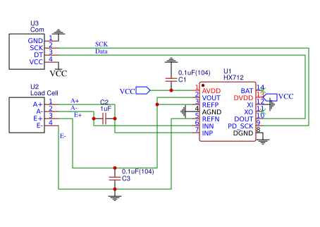
Started to solder a HX712 on a DIP board :) and tried to hook up. However, I am struggling a little bit getting a signal out of the HX712 (as you initially did):
- One positive thing is -> when I pull the SCK line low the HX712 “seems” to react by showing it readiness by pulling the DT line low (have not used the digital analyzer, but the setup is the same to the 711).
But here it ends ;( when I start pulsing the HX712 I do not get any read outs … I guess I did something “wrong” with my setup (please see the attached schematic). I would highly appreciate if you could “nudge” me to the right direction :)
Generally I omitted all the resistors (as above).
And here are my general questions regrading the pins:
-
AVDD and DVDD are connected (and have a stable power supply of 3.3V) -> What happens with the BAT pin -> in the manual it said to be connected to the higher of AVDD or DVDD but as you mentioned before I left it “floating”
-
I connected VOUT and REFP -> going to E+. E- goes to “AGND” and “REFN” ? Would that be correct? E- could directly connect to the AGND plane (same as AGND and REFN)?
The rest of the pins are self explanatory.
However, I do not understand what I did “wrong”. At least I must have done something wrong otherwise it would work :)
Do you have a hint on how measuring the differential voltage. I get a reading of 1.55 V on VCC to either INN or INP (both positive readings?)? REFP and REFN show 3.3V.
Are there any “measuring” points that would indicate a wrong setup or wrong wiring?
I would highly appreciate your help and look forward to your reply.
Best,
Chris.
Hi Chris,
So far, your wiring seems correct.
You can put BAT on the 3.3V line or leave it floating, i didn’t see any difference.
Your measures are indicating that you have wired the cell correctly as they give half supply voltage .
You can’t measure the differencial voltage, it’s far to small to be measured with regular voltmeters.
When in sleep mode, what voltage do you have on VOUT ? And in measure mode ?
You should have 0 V in sleep mode and a bit less than 3.3V when activated. This would tell you that the HX712 understands what you’ve send to it.
Check again wiring and code settings…
Patrick.
1 Like
Hi Patrick,
shame on me … I made a home PCB and while soldering I shorted the differential lines with the SMD cap :)…
The HX712 now produces pretty impressive measurements … My reference weight is 1054g and after calibration the weight fluctuates only ± 2 grams between 2sec measurements. Actually I have had not such a stable readout with the HX711.
And we are talking about a home made PCB and the load cells connected through a crappy bread board and the voltage supply through a USB TTL converter :)
But I can confirm that the HX712 256 gain is worth nothing! The readout is the same as with 128 gain … I get consistent readout but no improvement…
Great, now I can advance :) Thanks a lot!

1 Like
Sounds good ! ;-)
i Wish you good luck with your setup.
Patrick,
Hi there,
just wanted to let you know there’s an update on this at https://github.com/bogde/HX711/issues/39#issuecomment-480978218. @TK5EP, @clemens, @weef, @cpb.
Cheers,
Andreas.