Hi !
A happy new year to all on this forum ! A prosperfull beekeeping and building.
@weef
The 2.45V is what i had in memory when i tested these chinese HX711 boards. I have to check on one to confirm if this was the voltage i found on the cell…
Yes, as far as i remember, my prototype is using the on board PNP to switch a 5V supply. I can’t remember if i used this PNP to switch the output voltage or the ENABLE pin of a regulator. I think it’s this later solution.
My fault… i didn’t redraw the schematic after all my tests. I trusted my memory which i shouldn’t do anymore ! :-(
Thanks for the link to the datalogger. I already came across.
I modified my sketch and desactivated the A/D converter and brown-out, and my current dropped to 150uA.
I don’t have a spare digital pin to try to supply the DS3231. I will try to find a solution. But 'im not sure if it’s really worth it. The GSM is consuming a lot more each hour !
BTW, i was talking of a replacement for the DS3231 like the PCF2127 not a DS1307.
I’m actualy using 2 pins for each HX712. To free some pins, it might be possible to use one common pin for all four DOUT signals and one pin for each of the PD_SCK lines.
But i’m not sure it’s a good solution… It would wake up all 4 chips at the same time and supply all cells, consuming much more…
Have you made some tests with the DC filters you suggested ? What about the voltage drop across the resistors ?
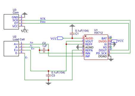
I see you are using the HX712 chip. I also ordered a couple of bare chips and dug into the data sheet. As already mentioned there seem to be a couple of unclear sections (one might deduct that the chip is not able to be set to a gain of 256 since it never appears in the electrical characteristics :( - although it is stated in the reading protocol. But before jumping into the details:
Does the HX712 give you any (real?) advantages over the HX711 (temp stability, etc?).
Now a couple of detailed questions:
I am struggling to set the correct AVDD and DVDD voltage (3.3V)? AV shall be <= DV … well Do you use an external voltage divider (as with the HX711 or not). In the reference setup AVDD and DVDD are fed from the same source?
I am having a hard time with the R1 - R4? How are they set? In terms of VOUt -> REFP / REFN they use R3 and R4 100Ohm? Would that be the same for 3.3V
Same question applies to the INP and INN resistors - why 200Ohm?
How do you set the correct resistors?
I highly appreciate your help and look forward to your reply.
My first choice for the HX712 was the advertised gain of 256. But it was a cruel finding that this chip has NEVER been designed for this gain. Confirmed by a mail from AVIA… “it’s a documentation bug that we will correct”… But after 2 years, nothing ! I would say this is a fraud !
I first thought that the library i modified for this usage was not working !
That said, i don’t see any real advantage using the HX712 compared to the HX711. Thermal stability seems to be worse, etc…)
Regarding your questions :
On DVDD, i use the same 3.3V voltage as my Arduino.
On AVDD i have 5V coming from a external clean stable regulator, so i have more voltage on the load cell.
R3-R4 are absolutely not needed, except for reducing the current through the cell ( 400 Ohm) . But they also introduce some voltage drop. I don’t use them.
R1-R2 and C2 are used as a DC filter to reduce noise. But with these values, i doubt they are very useful ? I don’t use them but increased C2 to 1uF.
The ONLY advantage i can see, is that the AVDD voltage is correctly switched with the internal transistor., but this can be done with the HX711 in a different way.
All in all, my boards are working fine but the next generation if any, will use HX711…
Started to solder a HX712 on a DIP board :) and tried to hook up. However, I am struggling a little bit getting a signal out of the HX712 (as you initially did):
One positive thing is -> when I pull the SCK line low the HX712 “seems” to react by showing it readiness by pulling the DT line low (have not used the digital analyzer, but the setup is the same to the 711).
But here it ends ;( when I start pulsing the HX712 I do not get any read outs … I guess I did something “wrong” with my setup (please see the attached schematic). I would highly appreciate if you could “nudge” me to the right direction :)
Generally I omitted all the resistors (as above).
And here are my general questions regrading the pins:
AVDD and DVDD are connected (and have a stable power supply of 3.3V) -> What happens with the BAT pin -> in the manual it said to be connected to the higher of AVDD or DVDD but as you mentioned before I left it “floating”
I connected VOUT and REFP -> going to E+. E- goes to “AGND” and “REFN” ? Would that be correct? E- could directly connect to the AGND plane (same as AGND and REFN)?
The rest of the pins are self explanatory.
However, I do not understand what I did “wrong”. At least I must have done something wrong otherwise it would work :)
Do you have a hint on how measuring the differential voltage. I get a reading of 1.55 V on VCC to either INN or INP (both positive readings?)? REFP and REFN show 3.3V.
Are there any “measuring” points that would indicate a wrong setup or wrong wiring?
I would highly appreciate your help and look forward to your reply.
So far, your wiring seems correct.
You can put BAT on the 3.3V line or leave it floating, i didn’t see any difference.
Your measures are indicating that you have wired the cell correctly as they give half supply voltage .
You can’t measure the differencial voltage, it’s far to small to be measured with regular voltmeters.
When in sleep mode, what voltage do you have on VOUT ? And in measure mode ?
You should have 0 V in sleep mode and a bit less than 3.3V when activated. This would tell you that the HX712 understands what you’ve send to it.
shame on me … I made a home PCB and while soldering I shorted the differential lines with the SMD cap :)…
The HX712 now produces pretty impressive measurements … My reference weight is 1054g and after calibration the weight fluctuates only ± 2 grams between 2sec measurements. Actually I have had not such a stable readout with the HX711.
And we are talking about a home made PCB and the load cells connected through a crappy bread board and the voltage supply through a USB TTL converter :)
But I can confirm that the HX712 256 gain is worth nothing! The readout is the same as with 128 gain … I get consistent readout but no improvement…